Introduction
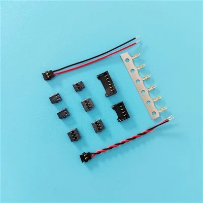
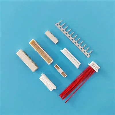
In the modern electronics landscape, miniaturization, reliability, and precision are paramount. From advanced automotive control units and medical diagnostic equipment to aerospace systems and consumer electronics, the demand for high-density, reliable internal connectivity solutions has never been higher. At the heart of many of these complex interconnect systems lies the wafer cable assembly. A wafer cable assembly-often integrating specialized connectors known as wafer connectors-provides a streamlined, secure, and space-saving method for transmitting power and data between printed circuit boards (PCBs) and internal system components.
Unlike standard, off-the-shelf wiring harnesses, custom wafer cable assemblies are engineered to meet specific electrical, mechanical, and environmental constraints. Designing and manufacturing these assemblies requires a meticulous, multi-stage process that combines advanced material science, precision engineering, automated machinery, and rigorous quality control. This article explores the comprehensive manufacturing process of custom wafer cable assemblies, detailing each critical phase from initial design and material selection to automated assembly, termination, and final testing. Furthermore, understanding this intricate workflow helps engineers and product developers optimize their designs for better manufacturability, cost efficiency, and long-term operational field reliability.
1. Design, Engineering, and Prototyping
The lifecycle of a custom wafer cable assembly begins long before any physical materials are cut or shaped. It starts in the engineering department, where design teams collaborate closely with clients to understand the exact application requirements and operational challenges.
Electrical and Mechanical Specifications
Engineers must evaluate several critical parameters during the initial design phase. These include voltage and current ratings, signal integrity requirements (such as impedance matching, shielding effectiveness, and crosstalk minimization for high-speed data transmission), operating temperature ranges, and environmental exposure factors like moisture, vibration, and chemical resistance. Mechanical constraints are equally vital; the routing path inside a device enclosure often dictates the length, flexibility, and outer diameter of the cable, as well as the orientation and pitch of the wafer connector itself. Additionally, factors such as insertion force, retention force, and space limitations within compact housings must be carefully calculated to ensure the assembly fits and functions perfectly.
Computer-Aided Design and Virtual Prototyping
Once the specifications are established, engineers use advanced Computer-Aided Design (CAD) and Electronic Design Automation (EDA) software to create detailed 3D models and 2D blueprints of the wafer cable assembly. These digital models allow the team to simulate routing, check for clearance issues, and verify that the selected wafer connectors and wire gauges fit seamlessly within the target hardware housing. Virtual prototyping significantly reduces development time and minimizes costly design flaws before physical production commences. Moreover, it enables engineering teams to run thermal and mechanical stress simulations, identifying potential points of failure and optimizing the design layout for maximum durability and performance.
2. Material Selection and Component Sourcing
The performance, longevity, and regulatory compliance of a custom wafer cable assembly depend heavily on the quality of the raw materials selected. Every component-from the individual conductors to the insulating jackets and the wafer connectors-must be carefully chosen to match the application environment.
Conductors and Insulation
The core of the cable assembly typically consists of stranded or solid copper conductors, often tinned or silver-plated to enhance corrosion resistance and solderability. The choice of conductor gauge (AWG) is dictated by current-carrying capacity, voltage drop limits, and flexibility requirements. Surrounding these conductors is the insulation material, which may include PVC, Teflon (PTFE), silicone, or cross-linked polyethylene (XLPE), depending on the thermal and chemical resistance needed. For applications requiring protection against electromagnetic interference (EMI) or radio frequency interference (RFI), shielding layers such as aluminum foil or tinned copper braiding are incorporated into the design. Furthermore, compliance with international environmental directives such as RoHS and REACH is strictly verified during this component sourcing phase to ensure hazardous substances are completely avoided.
Wafer Connectors and Terminals
The wafer connector serves as the crucial interface between the cable and the PCB. Selecting the right wafer connector involves evaluating the pin pitch (such as 1.0mm, 1.25mm, or 2.0mm for high-density applications), the number of circuits, locking mechanisms (friction lock or positive latching), and contact material. High-conductivity copper alloys plated with gold, tin, or palladium-nickel are commonly used for terminal contacts to ensure low contact resistance and high mating durability over thousands of insertion cycles. The housing plastics are also carefully selected for high thermal stability, flame retardancy (such as UL94V-0 ratings), and resistance to warping during surface mount or through-hole soldering processes on the PCB.
3. Wire Preparation and Precision Processing
Once the materials are sourced and inspected, the physical manufacturing process begins in the wire processing department. This stage transforms bulk wire reels into precisely cut, stripped, and prepared conductors ready for termination.
Cutting to Length and Wire Stripping
Automated cut-and-strip machines are utilized to handle high volumes of wire with extreme dimensional accuracy. These machines measure, feed, and cut the wire to the exact specified length required for the custom assembly. Simultaneously, the machine strips the outer insulation jacket and the inner conductor insulation to expose the bare copper strands to a precise length. Maintaining tight tolerances during this step is critical; even a fraction of a millimeter of exposed or damaged strand can compromise the integrity of the subsequent crimping process and lead to electrical resistance anomalies.
Pre-Treatment and Tinning
Depending on the specific design requirements, the exposed copper strands may undergo pre-treatment processes. For certain applications, the stranded wire ends are lightly twisted and ultrasonically welded or pre-tinned with solder to prevent strand fraying before insertion into crimp barrels or solder cups. This ensures a uniform cross-section and optimal mechanical stability during termination. Additionally, some high-end assemblies require specialized flux applications or laser stripping to remove delicate inner insulations without nicking the microscopic copper strands underneath, thereby maintaining absolute structural integrity.
4. Termination and Connector Assembly
Termination is one of the most critical stages in manufacturing a custom wafer cable assembly. It involves attaching the prepared wire ends to the metal contacts and housing them within the wafer connector body.
Automated Crimping
For the vast majority of modern wafer cable assemblies, mechanical crimping is the preferred method of termination. High-speed automated crimping presses use precision dies to press the metal contact terminal onto the stripped wire. A proper crimp creates a gas-tight mechanical and electrical connection, cold-welding the copper strands to the terminal barrel while providing strain relief on the wire insulation. Quality control systems, such as automated crimp force monitors, are integrated into these presses to measure pressure profiles in real-time, instantly rejecting any terminal that falls outside acceptable tolerances. These monitors track peak force, curve integration, and signature consistency to catch microscopic faults before assembly continues.
Housing Insertion and Assembly
Once the contacts are securely crimped to the wires, the individual terminals are manually or automatically inserted into the designated cavities of the wafer connector housing. The operators or automated insertion machines ensure that each contact clicks securely into place, engaging any internal locking tabs or latches designed to prevent back-out during mating. For multi-core or complex multi-branch cable assemblies, this stage may also involve bundling, twisting, or applying outer sleeves, braided mesh, or heat shrink tubing to organize and protect the wire runs leading up to the wafer connector. Secondary strain relief components, such as overmolding or cable ties, are frequently applied here to protect the termination zone from bending stresses.
5. Quality Control, Testing, and Packaging
Before any custom wafer cable assembly is packaged and shipped to the customer, it must undergo a comprehensive regimen of quality assurance and testing to verify its electrical performance and mechanical durability.
Electrical and Continuity Testing
Automated testing fixtures are used to check every single circuit in the wafer cable assembly. These testers perform continuity tests to ensure there are no open circuits or miswirings, and high-voltage (hipot) or insulation resistance tests to verify that there are no short circuits, pin-to-pin shorts, or insulation breakdowns. For assemblies designed for high-speed data transmission, specialized network analyzers may be used to test signal integrity, impedance, insertion loss, and crosstalk, ensuring that high-frequency data signals experience zero degradation across the connection line.
Mechanical and Environmental Inspection
In addition to electrical checks, sample assemblies from production lots often undergo rigorous mechanical testing. This can include pull-force testing to measure the tensile strength of the crimp connections, mating durability testing to ensure the wafer connector can withstand repeated connection cycles, and visual inspections using magnification systems or automated optical inspection (AOI) to check for cosmetic defects, correct pin configurations, and proper labeling. Environmental chamber testing, such as thermal cycling and humidity exposure, is also performed on prototype batches to guarantee field reliability. Once fully verified, the custom wafer cable assemblies are carefully packaged in anti-static bags or custom blister trays, labeled with comprehensive traceability data, and prepared for safe global shipment.
Conclusion
The manufacturing of custom wafer cable assemblies is a sophisticated discipline that bridges the gap between raw electrical components and high-performance electronic hardware. By combining rigorous engineering design, precise material selection, automated cutting and crimping technologies, and uncompromising quality control, manufacturers can deliver reliable interconnect solutions tailored to the unique demands of modern industries. As electronic devices continue to shrink in size while growing in complexity, the role of the custom wafer cable assembly remains indispensable, ensuring seamless, robust, and efficient connectivity across the technological landscape. Investing in expertly manufactured wafer cable assemblies ultimately guarantees superior system performance, reduced maintenance overhead, and long-term operational success for end-user applications.