Introduction
In the rapidly evolving landscape of modern electronics, the relentless demand for smaller devices with greater functionality has fundamentally transformed how internal components communicate, exchange data, and distribute power. As smartphones, medical gadgets, wearable technology, smart home appliances, and compact industrial controls shrink in physical profile, internal wiring must adapt to extreme spatial constraints. Traditional bulky cables, heavy-duty wire harnesses, and rigid point-to-point wiring methods are frequently no longer viable for high-density architectures. Instead, design engineers rely heavily on specialized micro-interconnect solutions to route power and signals safely and efficiently across crowded, highly optimized circuit boards.
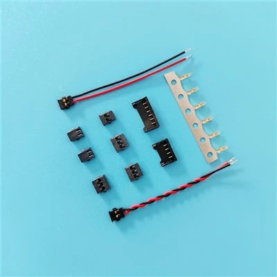
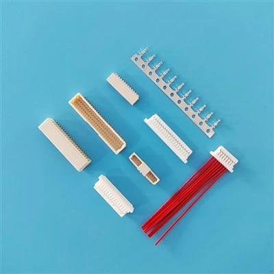
Among these sophisticated interconnect components, the concept of the micro-wire assembly often centers around specialized miniature connectors and matching cabling systems. While industry professionals frequently reference components like wafer connectors-which are low-profile male headers mounted directly onto printed circuit boards-the complete assembly paired with fine-pitch wiring is often broadly described or customized as a wafer cable system. Understanding how these micro-wire harnesses are structured, specified, tested, and deployed is essential for any engineer, technician, or designer looking to optimize internal device architecture, ensure signal integrity, reduce electromagnetic interference, and streamline manufacturing assembly from prototype development to full-scale mass production.
1. Defining the Wafer Cable and Micro-Wire Architecture
To fully grasp what a wafer cable represents, one must examine its core anatomical components, materials science, and engineering foundations. At its simplest, this type of assembly is a wire-to-board harness where fine-gauge stranded or solid copper wires are mechanically crimped to miniature metal terminals using high-precision automated machinery. These terminated wires are then inserted into a polarized plastic housing, often referred to as a connector housing or receptacle, which is designed to mate smoothly and securely with a corresponding printed circuit board mounted wafer header.
The term "wafer" in this context primarily originates from the low-profile, flat-base header style that solders onto the surface of the circuit board, providing a secure, low-height landing zone for the incoming cable plug. Unlike bulky multi-pin round connectors or heavy cylindrical interfaces, a wafer cable assembly focuses heavily on horizontal or vertical space-saving efficiency, allowing components to sit flush against one another. The pitch-the precise distance measured from the center of one conductive pin to the center of the adjacent pin-is exceptionally narrow, commonly ranging from ultra-fine 1.0 millimeter down to 0.8 millimeter, 0.6 millimeter, or even 0.4 millimeter in extreme miniaturization scenarios. This micro-pitch capability allows dozens of independent signal and power lines to occupy a physical footprint smaller than a fingernail, making it an indispensable asset for modern dense circuit layouts where every square millimeter of board space is fiercely contested. Furthermore, the internal cabling often incorporates specialized shielding tapes, foil wraps, or internal drain wires to minimize electromagnetic interference across high-speed data lanes, ensuring that high-frequency signals do not degrade when routed near noisy power supplies or switching regulators.
2. Key Advantages of Micro-Wire Harnesses in Electronics
Deploying a precision micro-wire harness system offers numerous mechanical, electrical, and manufacturing advantages over traditional hand-soldered wiring or bulkier connector alternatives in compact technical applications.
First and foremost is exceptional space optimization. In applications like ultra-thin laptops, handheld test equipment, high-definition action cameras, and compact drone gimbals, vertical clearance is severely restricted. Low-profile housing geometries and fine-wire bundles ensure that internal routing does not obstruct vital airflow paths or interfere with adjacent moving mechanical components. Second, these assemblies deliver highly reliable mechanical polarization. Polarized housings feature specific physical keying, chamfered edges, or asymmetrical side walls that make it physically impossible to plug the cable in backward or upside down, completely eliminating costly assembly errors during factory production, rework procedures, or field maintenance operations.
Furthermore, prefabricated micro-wire harnesses significantly enhance manufacturing efficiency and operational scalability. Instead of requiring factory technicians to manually strip, flux, and solder individual miniature wires directly onto a printed circuit board-a tedious, highly repetitive process prone to cold joints, flux residue contamination, and human error-a pre-assembled cable allows for quick, modular plug-and-play installation. Many configurations also feature integrated friction locks or positive latching mechanisms that emit a distinct tactile and audible click upon complete mating, securing the connection against accidental dislodgement caused by everyday vibrations, repetitive mechanical shocks, or thermal expansion cycles. This modular approach also simplifies field servicing, enabling technicians to swap out damaged sub-assemblies in minutes rather than replacing an entire device.
3. Core Technical Specifications to Evaluate
Selecting or designing the correct micro-wire harness for your project requires careful, methodical evaluation of several critical electrical, mechanical, and environmental parameters to prevent unexpected field failures and ensure long-term system reliability.
Current and Voltage Ratings: Due to the extremely small cross-sectional area of micro-wires, which often range from 28 AWG down to 32 AWG or even finer gauges, the current-carrying capacity is inherently limited. Exceeding the ampacity limit can cause excessive Joule heating, rapid insulation breakdown, or conductor fatigue. Engineers must always verify the manufacturer's thermal derating charts, taking into account ambient operating temperatures and the total number of energized circuits packed within the same housing.
Wire Gauge and Insulation Materials: The choice of conductor insulation-such as polyvinyl chloride, fluorinated ethylene propylene, Teflon, or silicone-dictates the overall flexibility, temperature resistance, and chemical durability of the cable. Highly flexible insulation is critical if the harness must bend tightly around internal chassis corners during tight mechanical integration without kinking or stressing the crimp joints.
Mating Durability and Retention Force: Consider how many times the cable will be plugged and unplugged over its operational lifecycle. Consumer electronic devices might only require a handful of mating cycles, whereas modular diagnostic tools and laboratory instruments demand high-endurance contacts plated with gold or durable tin alloys to maintain low contact resistance over thousands of insertion and withdrawal cycles.
Environmental Sealing and Plating Selection: Depending on whether the device operates in a clean office environment or a corrosive industrial setting, contact plating materials must be chosen wisely. Gold plating prevents oxidation in sensitive low-current data lines, while tin plating offers an economical solution for robust power delivery connections where wiping action cleans the contact surface during mating.
4. Advanced Manufacturing and Quality Control Processes
The production of high-reliability wafer cables and micro-wire assemblies requires state-of-the-art manufacturing techniques and stringent quality assurance protocols. Because the components are microscopic, manual assembly is virtually impossible to scale reliably. Instead, automated cut-strip-terminate machines handle the precise preparation of fine-gauge wire strands. These machines strip the insulation with micron-level accuracy and crimp the tiny metal terminals onto the bare conductor in a single, flawless motion, ensuring a gas-tight joint that resists oxidation and mechanical fatigue.
Quality control measures in this sector are exceptionally rigorous. Automated Optical Inspection systems and high-magnification digital microscopes scan crimped terminals for structural defects, such as stray wire strands, incomplete insulation grip, or barrel deformation. Electrical continuity testing rigs verify that every single circuit within the multi-pin harness is correctly mapped and free from opens, shorts, or intermittent contact faults before the assemblies ever leave the factory floor. Furthermore, pull-force testing is routinely performed on sample batches to guarantee that the mechanical retention strength of the crimp and the housing lock meets or exceeds international industry standards. Environmental stress screening, including thermal shock and vibration testing, is also applied to validate assembly resilience under harsh operating conditions.
5. Common Industry Applications and Use Cases
The remarkable versatility, compactness, and reliability of fine-pitch wire assemblies mean they are integrated across a remarkably diverse spectrum of high-tech industries and specialized hardware sectors.
In the realm of consumer electronics, compact displays, internal camera modules, touch panels, and advanced battery management systems rely heavily on micro-wire connections to bridge separate rigid circuit boards without adding thickness to the sleek device casing. In the automotive sector, advanced driver-assistance systems, dashboard infotainment clusters, steering wheel control modules, and seat adjustment sensors utilize miniaturized wiring to handle complex sensor feeds within cramped spatial envelopes. Meanwhile, the medical device industry depends critically on these reliable, space-saving harnesses for portable diagnostic tools, patient-monitoring sensors, ultrasound probes, and handheld therapeutic instruments where absolute electrical stability, biocompatibility, and user safety are of paramount importance. Additionally, industrial automation equipment utilizes these cables in compact sensor nodes and robotic arm joints where repetitive motion requires high flexing endurance.
Conclusion
The wafer cable and its associated micro-wire harness ecosystem represent an absolute cornerstone of modern compact electronic design. By bridging the gap between ultra-dense printed circuit boards and external sub-assemblies, these low-profile interconnect solutions enable engineers to pack incredible processing power, sensing capabilities, and advanced functionality into ever-smaller physical form factors without sacrificing structural integrity.
Mastering the rigorous selection criteria-ranging from precise pin pitches and wire gauges to current limits, thermal derating, and locking mechanisms-ensures that your electronic assemblies remain durable, efficient, and reliable under demanding operational conditions. Ultimately, treating internal cabling as an engineered critical path rather than an afterthought will safeguard your project's performance, streamline manufacturing workflows, reduce warranty claims, and deliver a robust product capable of standing the test of time across its entire operational lifecycle.